
Advanced Material Applications Become the New Key to Packaging and Testing
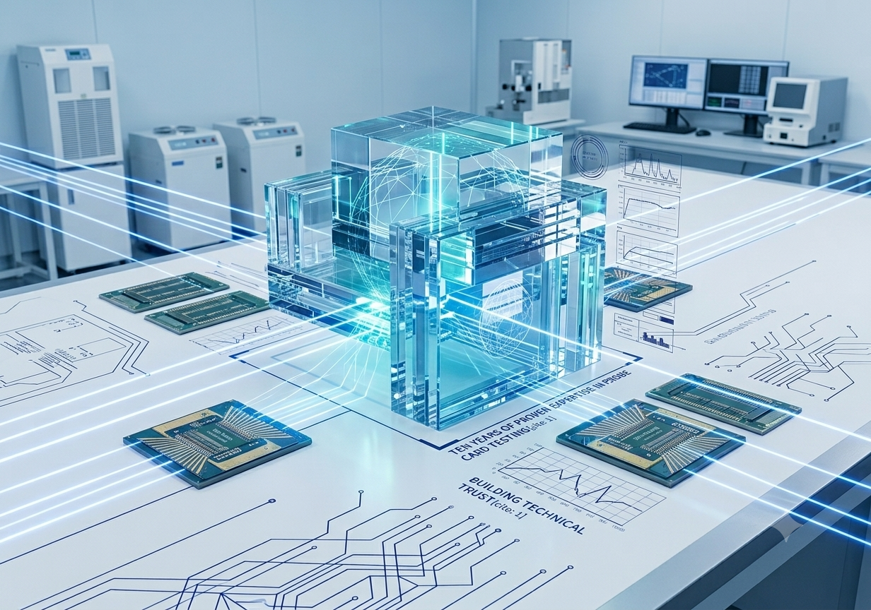
Driven by the exponential growth in demand for AI computing power, the semiconductor industry's focus is shifting from pure process scaling to heterogeneous integration and material innovation. Industry experts point out that as chip stacking density continues to increase, thermal dissipation efficiency and signal stability are becoming the core dimensions of competitiveness in packaging and testing.
Challenges and Opportunities in Heterogeneous Integration
While high-performance computing (HPC) chips widely adopt advanced packaging, thermal effects and physical interference frequently impact overall stability during complex computational tasks. Sharing insights at an industry seminar, New Ray Innovation emphasized that material-level optimization can effectively mitigate noise issues in high-frequency signal transmission—a critical bottleneck that many IC design houses urgently need to resolve during mass production.
Pioneering Technology to Build Solid Technical Trust
With long-term commitment to probe card R&D and testing, New Ray Innovation has not only overcome the manufacturing hurdles of miniaturized probes but also expanded its technological reach into specialized material applications. The company stated that it will continue to deepen collaborative design (Co-design) with upstream supply chain partners, translating test data into valuable insights for process improvement. This enables clients to accelerate time-to-market and stay ahead in the fiercely competitive global chip market.